
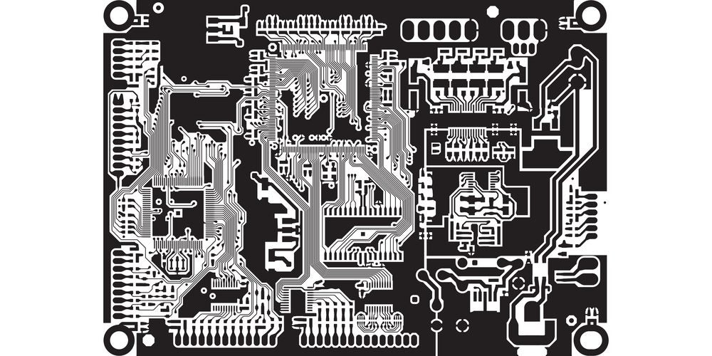
IPC is a global trade organization working to create consistency in the electronics industry. IPC standards are not limited to physical objects; however, multiple separate standards exist simply for naming things. The organization has published many standards over the years governing electronics design, manufacturing, assembly, and quality testing. There are more than 10 separate IPC standards for PCB design alone, including IPC naming conventions specifically for components.
When we talk about standards and IPC naming conventions, we are really referring to standardized methods for naming packages and footprints for components, rather than assigning MPNs to components from different manufacturers. Manufacturers will have their own naming and part numbering conventions for their components, which are meant to denote product line, application area, some physical dimensions, and feature sets. In contrast, IPC conventions focus on standardized packages used for SMT and through-hole components.
Two IPC Naming Conventions
IPC standards cover every facet of electronics design and fabrication, including materials, assembly, components, and layout. IPC naming convention standards are a specific subset of these standards, describing how certain types of electronic components should be named. There are two major naming standards that apply to PCBs:
- IPC-7351B: Generic Requirements for Surface Mount Design and Land Pattern Standard
- IPC-7251: Generic Requirements for Through-Hole Design and Land Pattern Standard
Many PCB design tools are built with component creation tools, which help you comply with the most recent revisions of the IPC standards. Some design platforms include built-in component generators that will create a compliant PCB footprint as well as a compliant name under IPC 7351B or IPC-7251. Of these two naming conventions, IPC-7251 is more complex, since it refers to other established IPC standards to determine part of its naming scheme.
Through-Hole Names Under IPC-7251
IPC-7251 names through-hole components by starting with the component type (e.g., polarized capacitor, fuse, etc.). The first 3-6 characters in a standardized IPC-7251 name describe the component type, orientation, and mounting style (vertical, horizontal, right angle, etc.). If the component is a capacitor, this character group also includes its polarity. The rest of the name includes the component dimensions and complexity.
Under IPC 7251 standards, component dimensions are defined in millimeters, with two places to the right of the decimal point and no leading zeros. Part of an IPC 7251-compliant name is the component’s fabrication complexity level. This is defined using either “A”, “B”, or “C”, which matches the Design Producibility levels listed in the IPC-2221 and IPC-2222 standards. In addition, IPC-7251 further references IPC 7252-7259 for different types of components, connectors, and mounting hardware.
The IPC naming convention for through-hole land patterns uses component dimensions to derive the land pattern name. The first 3–6 characters in the land pattern name describe the component family, which is then followed by the following data:
- P = Pitch for components with more than two leads
- W = Maximum lead diameter
- L = Body length (horizontal mounting)
- D = Body diameter for round components
- T = Body thickness for rectangular components
- H = Height for vertically-mounted components
- Q = Number of pins for components with more than two leads
- R = Number of rows (for connectors)
- A, B, or C = Fabrication complexity level
A similar format is used in the IPC naming convention for SMD components.
SMD Names Under IPC-7351B
IPC-7351B names surface-mounted components by starting with the component dimensions and land pattern; there are specific codes included in the standard for different component packages. The first 3-7 characters in a standardized name are either an acronym of the component type or an abbreviation that distinguishes between component subtypes. The rest of the name varies by component, but the overall component name is related to the part’s land pattern.
Some components include their dimensions in metric units within their name. When the name includes dimensions, those dimensions have one significant digit on each side of the decimal point. Other IPC-7351B names contain pin numbers or denote the presence of specific features. For example, ball grid arrays include a “C” within their name for collapsing balls, or “N” for non-collapsing balls. An example of a BGA120C80P10X12_900X1100X100 ball grid array package is shown below.
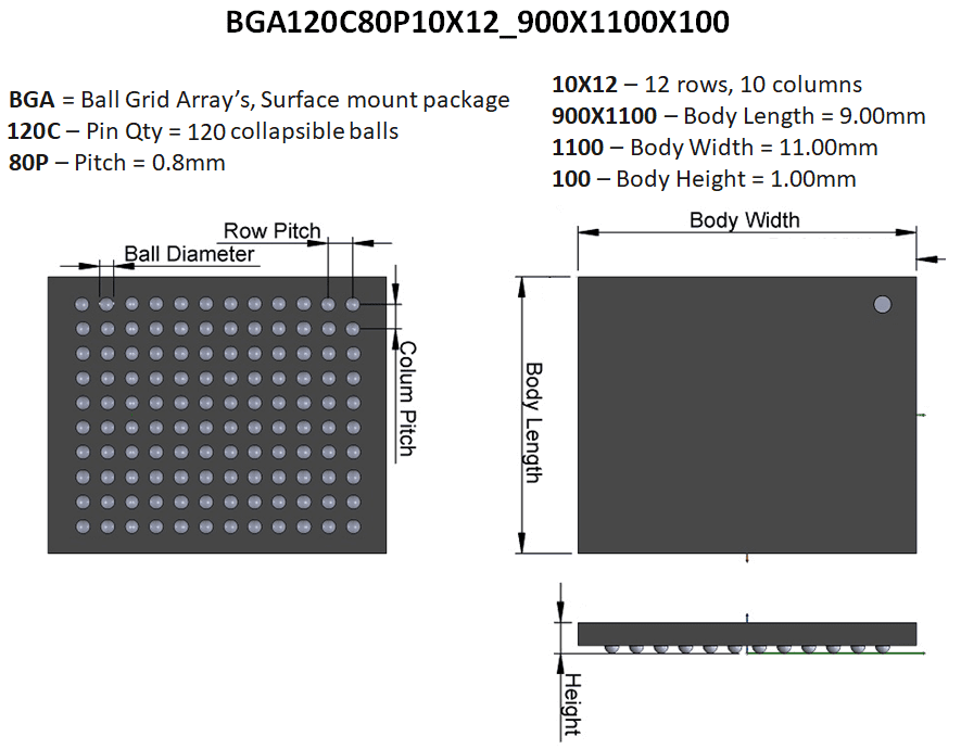
The example above is one example of the structure used to create naming conventions for SMD components. Although the naming format shown above does not apply to every package and land pattern, there is a general pattern that one can extract for a range of components. The naming convention follows the general pattern:
(Package type) + (Lead type) + (Lead pitch) + (Body length) + (Body width) + (Height)
Some components may also have a suffix at the very end of the component name to indicate things like heat sink attachment, reversed pin orders, or non-standard pins for transistor footprints.
Here, we’ve only looked at the land pattern for different components, which will need to be reflected in the PCB footprint. We still haven’t looked at the padstack, which has its own IPC naming conventions.
Padstack Naming Conventions
Padstack information is also important to consider when working with component models and creating your PCB footprints. Although padstacks are part of the IPC-7351 and IPC-7251 naming conventions for use in PCB footprints, they are also specified in the PCB layout when vias are used to route through multiple layers. Your design tools will normally create padstacks automatically during layout as you place and size vias.
The padstack naming convention consists of combinations of letters and numbers that represent the shape and dimensions of landing pads on different layers. The first letter defines the shape of the pad, and the following number designates the pad size. The letter “h” is normally used to indicate the presence of a hole, followed by a number for the hole diameter. If you use modern PCB software and you start placing vias in the layout, the software might start creating padstack templates with names that match the IPC naming convention.
For a complete list of component prefixes and abbreviations under both standards, take a look at this document. To see a full list of guidelines for naming padstacks, see this document. As of now, everything is still named under the IPC-7251 or IPC-7351B standards. There is still no release date for IPC-7351C, which would be the newest revision on naming conventions for SMD land patterns. No matter which standard you are using, the right set of component search tools can help you quickly find new components and import them into your design.
Ultra Librarian provides components that adhere to IPC naming conventions whenever possible. Additionally, our data is stored in a vendor-neutral format, ensuring there are no inconsistencies across CAD types. Working with Ultra Librarian takes the guesswork out of preparing for your next great device and puts your ideas on the road to success. Register today for free.


