
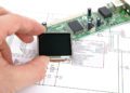
Board-level tests are often used to identify suspect electronic components
Every circuit board should go through some testing before and after it comes off the assembly line. The goals of testing are varied, and there is a huge number of tests one could perform for any circuit board. The specific tests required for a particular circuit board depend on the application and the environment where the board will operate. Of all the tests that can be performed for a PCBA, component testing is arguably the most important.
Component manufacturers take great pains to identify and remove bad components from their stocks before they enter the supply chain, but sometimes a bad batch will slip into distribution. It is important to understand how to identify faulty electronic components as well as how to distinguish them from a board-level failure. In this article, we’ll detail some ways you can distinguish board-level and component-level failures and some of the basic tests used to evaluate electronic components.
How Do You Identify Faulty Electronic Components?
Faulty electronic components can be identified in three stages during a project:
- Before fabrication
- During assembly
- During functional testing after a PCBA is received
Manufacturers know how to identify faulty electronic components using a set of standard tests. However, while semiconductor companies do their best to remove faulty components from production lots and manufacturers help eliminate premature failures with testing, it is largely up to test engineers or designers to identify faulty components. Once a board is received, the boards should go through a round of qualification testing to identify any failed boards. These failed boards are then investigated for any possible failed components.
Identifying Faulty Components During Manufacturing
Burn-In Testing
One important test that can be performed before manufacturing is burn-in testing. This involves bringing a batch of components up to a very high temperature, powering on the components, and letting them run until they are allowed to fail. Because this process involves large batches of components, it is only performed in high-volume runs with the goal of removing the components with the shortest possible lifetime.
While this type of accelerated life test is only done in high-volume production runs, in-circuit testing can be performed during assembly with the goal of identifying board failures.
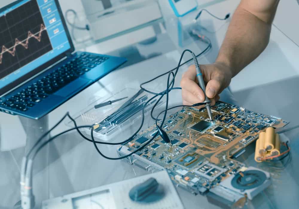
In-Circuit Testing
In-circuit testing is performed with the board powered up using a flying probe machine or bed-of-nails tester. In this type of testing, an automated machine probes the voltage and current on important nets to be measured during assembly, and the electrical measurements are compared with intended design values. To ensure your manufacturer can properly identify a faulty board or component during assembly, it’s best to place test points on the PCB around important components for in-circuit testing.
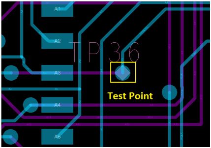
Test points are placed as small pads in your PCB layout
If the measurements don’t match the values calculated from the design, then the boards can be pulled and inspected further. Further testing will often be required to diagnose whether there is a board-level or component-level failure. This allows failed boards to be identified and inspected before they are sent out to the end customer.
Identifying Faulty Components During Board Bring-Up
Identifying a faulty electronic component during board bring-up can be more difficult. A single bad component can cause a board to work incorrectly or fail to work entirely, but it is not immediately obvious whether any such failure is due to a component. The problem could be linked to an assembly defect, a fabrication mistake, an incorrect footprint, or a specific component.
In this type of device inspection and debugging process, designers need to probe along the problem interconnect and try to identify the specific point where the failure occurred. The component that appears to be faulty on an assembled board may not be the component that is responsible for the problem; it could be a different component along that signal path.
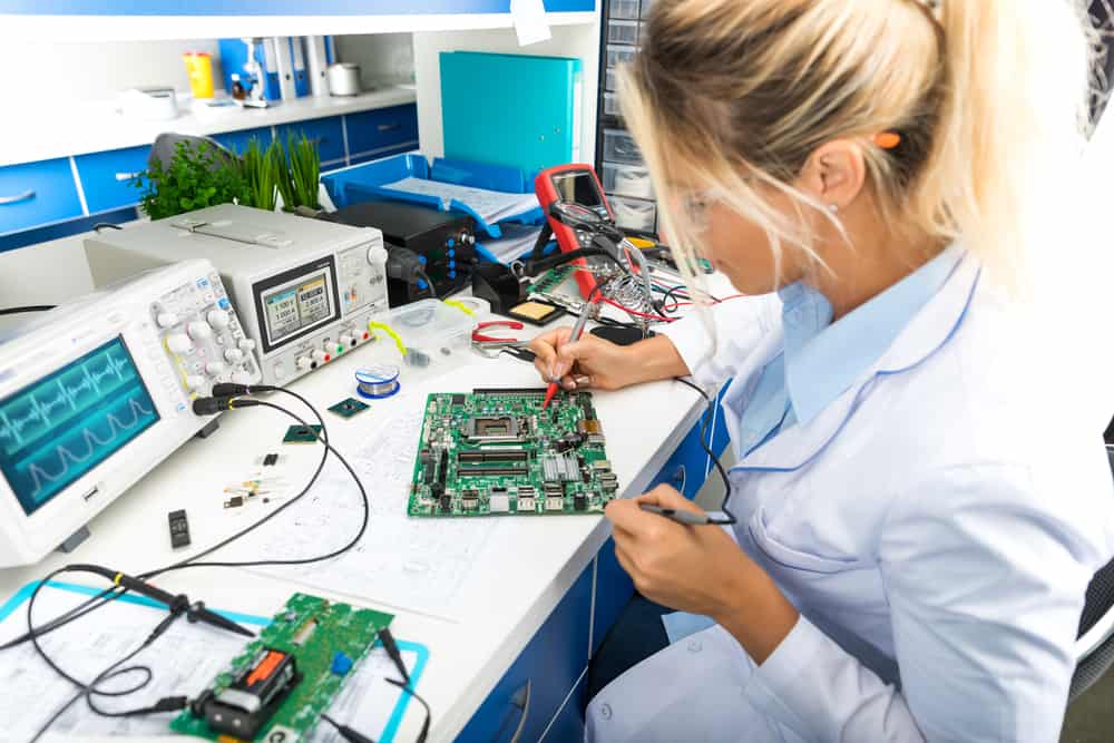
Unless specific test fixtures are placed on the board, a test engineer will need to manually probe important connections to determine whether a board failure is due to a failed component or a manufacturing defect
This type of unclear failure is most common and requires more investigation. If the suspect component is found to be functioning correctly, then the problem lies somewhere in the design data or it occurred during manufacturing. If, after further inspection, there are no defects in the bare board or assembly, then the problem might be as simple as an incorrect footprint.
Incorrect Pinout or PCB Footprint
If the problem is narrowed down to an incorrect pinout or footprint in the CAD data, then expect all the boards in that lot to be functioning incorrectly. Fixing this problem requires extensive rework or scrapping the entire production run. In some cases, you might be able to replace the problem component with a variant with a matching footprint and correct pinout. Make sure to verify all footprints when creating the PCB layout and, if possible, only use footprints that are verified from the component manufacturer.
The case of an incorrect pinout with matching land patterns does not happen often, as many components are designed to be drop-in replacements. However, to ensure you’re always using correct footprints, use an electronic parts search engine to find verified footprints, schematic symbols, and sourcing data for your design.
When you need to find ECAD models that are verified by component manufacturers, try using the electronics search engine features in Ultra Librarian. If you’re debugging a design and you need to identify faulty electronic components, you’ll be able to access verified CAD data supplied by manufacturers to use for comparison with your footprints and for updating your designs. All CAD data is compatible with popular ECAD applications and will help you streamline your verification process.
Working with Ultra Librarian sets up your team for success to ensure streamlined and error-free design, production, and sourcing. Register today for free.

