
Different types of PCBs carry a diverse range of design rules, layout schemes, and sets of components. New designers may not realize that there are generally different types of PCBs, but the same overall process is used to create a PCB layout and other CAD documents in ECAD software. If you’re a new designer and you’re exploring the various types of PCBs you can create for a new design, it helps to understand the general design process and how to select components for your design.
The Different Types of PCBs and Their Construction
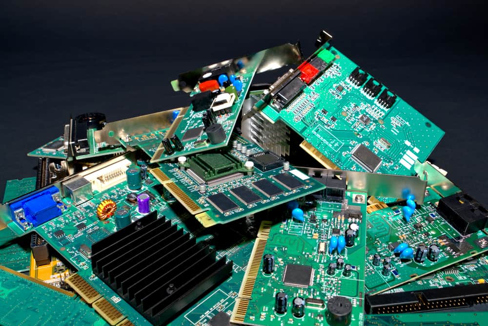
All circuit boards follow the same design process, but they can be built on different stackup constructions and material platforms. The primary factors distinguishing different types of PCBs are their stackup construction, layer count, rigidity, and dielectric material. Circuit boards can be classified into several areas based on these factors, as shown in the table below.
| Single-sided | A rigid PCB where components are assembled and soldered on only one side of the PCBA. Typically only the component side has silkscreen.
Material platform: Epoxy + fiberglass resins |
| Double-sided | A rigid PCB where components are assembled and soldered on both sides of the PCBA. Both sides will have silkscreen.
Material platform: Epoxy + fiberglass resins |
| Multi-layer | Multi-layer PCBs stack multiple rigid dielectric layers with internal copper plane layers.
Material platform: Epoxy + fiberglass resins |
| Rigid-flex or flex | A rigid-flex PCB is a multi-layer board that includes a flexible region attached to one or more rigid regions. Flex boards only have flexible materials.
Material platform: Epoxy + fiberglass resins (rigid-flex only), polyimide for flexible regions |
| Metal-backed | These boards use a sheet of metal as the backing material for a single-sided PCB.
Material platform: Epoxy + fiberglass resins, copper or aluminum |
| Metal-core | A PCB that has a metal sheet (normally aluminum) as a core layer. This type of board is generally single-sided, but it can be double-sided.
Material platform: Epoxy + fiberglass resins, copper or aluminum |
| Radio frequency | A rigid PCB constructed from specialized PTFE-based or PPE-based dielectrics that have lower losses than FR4 substrates at high frequencies.
Material platform: PTFE/PPE + fiberglass resins and bondplies |
Generally, overseas manufacturers that are interested in competing on price still distinguish between single-sided, double-sided, or multi-layer PCBs. However, today’s modern PCBs are typically double-sided multi-layer PCBs; there is no need to continue distinguishing between these types of boards. Most manufacturers can handle any of these types of PCBs without problems and will generally be able to accommodate any material rated as an FR4 dielectric by NEMA and that conforms to an IPC-4101 slash sheet. More specialized materials like Rogers (PTFE + fiberglass), Megtron (PPE + fiberglass), or flex boards using polyimide materials require more specialized processes.
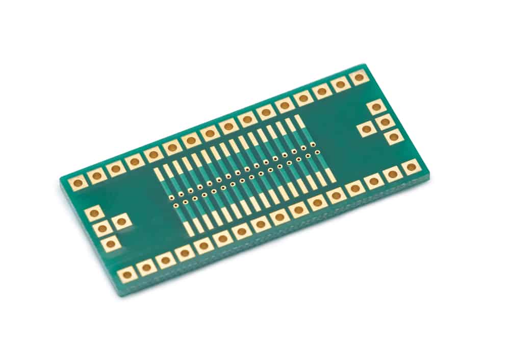
Rigid boards will use the same FR4 laminate materials used in this SMD-to-DIP adapter board
Once a material platform and board assembly type are selected, all designs follow a simple process:
- Create circuits and schematics, including selecting materials for the design.
- Import component models into the PCB layout.
- Route connections between components in the PCB layout.
- Generate final artwork and output files for fabrication and assembly.
Some guidelines on different types of PCBs state that designs need to be classified based on the types of components used in the design (i.e., SMD vs. through-hole components). With modern assembly processes, there is no need to classify boards as only using surface mount vs. through-hole components. Many boards will contain both types of components, and PCB assembly houses understand how to accommodate multiple soldering processes used for each type of component.
Where Can You Find Components for Your Board?
When floorplanning different types of PCBs and creating your circuits, you’ll need to find components to use in the design to produce your desired functionality. When PCB designers talk about finding components, they aren’t talking about looking through distributor websites to buy components. Instead, designers are looking for accurate PCB footprints and schematic symbols for the components they need. These CAD objects are placed in schematic drawings and the PCB layout so that the physical design of the board can be completed.
Designers have a few strategies they can use to find or make CAD data for components in different types of PCBs:
- Design all footprints and symbols from scratch. This can be done in-house, through a contractor, or through a component creation service. While this is a low-risk option, creating CAD data from scratch for each project takes a lot of time and leads to a lot of repeated work.
- Only use components with common footprints. This means designers are only using components that have standardized packages (e.g., SOT packages for transistors). Unfortunately, most ICs will need to have their CAD data created from scratch because nearly every pinout on an IC is unique.
- Find footprints online. There are some community websites where symbols and footprints can be downloaded for free. Unfortunately, these are not always verified by the manufacturer or other designers, and there may be some mistakes in the footprints or symbols.
If the component footprints and symbols are incorrect, there is a risk the pad/hole placement in the board does not match the real component that will be placed during assembly. This might sound like a simple problem to spot, but a small error in pad arrangement can mean a board will not pass through assembly. New designers should take care to find some resources where they can find verified footprints, schematic symbols, and sourcing data for their designs.
When you need to find ECAD models for different types of PCBs that are verified by component manufacturers, try using the electronics search engine features in Ultra Librarian. If you’re debugging a design and you need to identify faulty electronic components, you’ll be able to access verified CAD data supplied by manufacturers to use for comparison with your footprints and for updating your designs. All CAD data is compatible with popular ECAD applications and will help you streamline your verification process.
Working with Ultra Librarian sets up your team for success to ensure streamlined and error-free design, production, and sourcing. Register today for free.


