
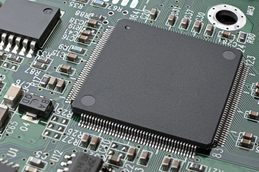
PCB assembly with SMT components
Since the early days of electronic circuit board assembly, virtually all components were attached using what is known as through-hole technology (THT). This technology does have advantages and is still in use today. However, as component manufacturing capabilities advanced and the demand for smaller electronic devices and products increased, the need for more compact—yet functional—components emerged. The answer, surface mount technology (SMT), has largely replaced or at least provided an alternative to THT components in most cases.
The proliferation of surface mount devices (SMDs) on circuit boards has impacted more than board and final product sizes. In fact, the use of SMT influences the entire manufacturing stage of PCBA development, which includes fabrication and assembly. Fabrication is the initial physical embodiment of a printed circuit board (PCB) without components. During this stage, the board’s surface layout(s), stackup, and other physical parameters are constructed. Assembly, the final manufacturing stage, is where components are attached. To fully understand how SMT components affect board assembly, it is important to understand how they differ from THT components as well as the steps that comprise PCB assembly.
THT vs. SMT Components
Both THT and SMT components may be active or passive devices. One obvious difference between through-hole components and surface mount components is size, with through-hole parts typically being larger and some SMDs being quite small (for example, a 0402 resistor is only 1 mm x 0.5 mm). This does not necessarily mean they require more surface space on the board. For example, THT capacitors are often much taller and demand more space in the vertical direction as opposed to similar SMT capacitors.
Through-hole components invariably require more space within the board itself, as they require plated through-hole (PTH) vias that extend from the top surface to the bottom (or back) surface of the board. SMDs, on the other hand, may or may not require vias. When vias are required—for example, when ball grid array (BGA) and quad flat no-leads (QFN) parts are used—they are either microvias, blind, or utilize via-in-pad (the most difficult via option to implement for most CMs) options. Other SMD packages, such as small outline packages (SOPs) and small outline ICs (SOICs), have pins that protrude from the part to the board surface. Depending on your layout, vias may or may not be required.
In addition to the above, your choice of components greatly impacts the following design considerations:
- Board strength
- Number of layers in the stackup
- Amount of clearance needed between components
- Enclosure size
These are just a few of the major design issues you must address depending on whether you opt to use through-hole or surface mount parts. Another major consideration is how your board will be assembled.
The PCB Assembly Process
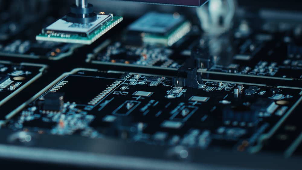
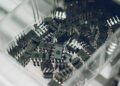
Example of a picked SMT component during PCB assembly
PCB assembly is the critical final process in building your boards and, therefore, your assembler has the responsibility of ensuring that the finished product meets your requirements. This stage of manufacturing includes a number of inspections and verifications as well as the following basic steps:
- Prepare for soldering by applying solder paste.
- Pick the correct part.
- Place component accurately on the footprint.
- Solder components in place.
- Check solder joint connection quality and make corrections, if necessary.
- Clean excess debris from the board.
- Depanel boards into single units for packaging and shipping.
The list of steps above is applicable irrespective of the components used. The primary variance is the soldering process implemented by your CM. For THT, the process is almost always wave soldering. However, for SMT components, the process is a bit more involved.
How SMDs Affect Board Assembly
When soldering surface mount components, reflow ovens are typically used as wave soldering and may not provide accurate coverage for small, fine pitched components. The reflow process allows sufficient time for the solder to reach all necessary areas as well as temperature control. The fact that many SMT packages require the use of vias also means internal board inspection is necessary, which is not as critical for THT components. SMDs are also subject to solder bridging, which is when one side of the component becomes detached and rework is required.
Another important factor that should influence your choice of component technology is the type of design. As an example, for high-power applications, you may want to go with through-hole components, as these devices tend to be heavier and require stronger attachment, which through-hole vias provide. On the other hand, SMT components are more lightweight and are only attached to the board surface. This means they are more likely to be displaced in environments where vibration and/or constant motion are present. In these situations, it may be necessary to add supports to ensure that SMDs are maximally secured.
Even with these considerations for PCB assembly, the advantages of smaller boards and products, more complex design capability, and lower costs make SMT components very attractive for PCBA and electronic product development.
If you’re looking for CAD models for common SMT components, Ultra Librarian helps by compiling all your sourcing and CAD information in one place.
Working with Ultra Librarian sets up your team for success to ensure streamlined and error-free design, production, and sourcing. Register today for free.
