
The complexity of today’s PCBAs means separate design and manufacturing experts are needed to produce the boards that our electronic systems, appliances, industrial equipment, vehicles, ships, and aerospace platforms require. However, for a smooth process from start to finish, both designers and manufacturers need to have a basic understanding of what the other does. When designers understand the PCB assembly process, they can make decisions that aid their CM in making the highest-quality boards.
Understanding the PCB Assembly Process
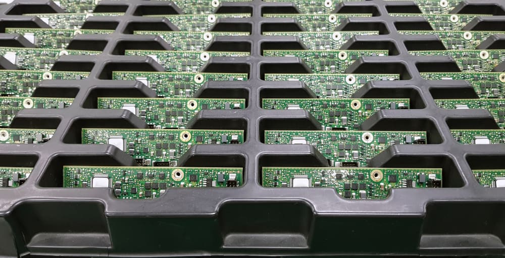
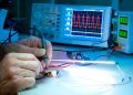
PCB assembly is the final activity performed during circuit board manufacturing (the other is fabrication) and can be defined as follows:
| The PCB assembly process, performed after bare board fabrication, is where the components selected during design and listed in the BOM are attached to the PCB through a soldering process—such as wave, selective, or reflow—depending on the type and size of components used. |
As expressed above, the major objective during PCB assembly is to attach THT and/or SMT components. However, as the final process during manufacturing, assembly is also when inspections (for example, automated optical inspection), testing (such as flying probe or other in-circuit tests), cleaning, conformal coating or other protections, and depanelization are performed. Although the CM actually implements these tasks, the decisions that you make during the design process can greatly impact the quality of the boards built.
Designing to Aid PCB Assembly
For a long time, engineers and PCBA designers worked with very little, if any, knowledge of how their boards were actually built. This black-box manufacturing paradigm was the source of a myriad of problems that translated into designs that were not manufacturable, the inability to get accurate quotes, exceptionally long turnaround times, and increased costs. Fortunately, this inefficient PCBA development process has been largely replaced with a white-box approach that recognizes the importance of transparency, collaboration, and following your CM’s design for manufacturing (DFM) rules.
Transparency here means that you should have an understanding of how your design choices impact the board build process, especially PCB assembly. Additionally, engaging your CM so that your design intent is known will enable your manufacturer to offer advice and institute changes that will enhance your board’s quality while still meeting your performance objectives.
Guidelines to Improve the PCB Assembly Process
A set of good practices to aid you in helping your CM’s PCB assembly process is listed below.
- Optimize the component selection process.
Avoid using exotic components, which can be hard to find and may slow your board build process down. Additionally, unless both are necessary, opt for THT or SMT components. - Do not overload nets.
Overloaded nets translate into heavy copper weights on your board, which may require wider traces and may present clearance challenges. - Follow component, trace, and edge clearance rules.
Clearances serve to ensure that soldering and depanelization can be performed easily. Moreover, lack of clearance can also introduce EMI problems that will impact operation and performance. - Use a sufficient, but minimum, number of layers in your stackup.
Extra layers increase the board height, which not only impacts enclosure design, but can also add material costs to high-volume production orders. - Perform DFA and DFM checks often.
You should strive to clear all DFM and DFA violations, which is much easier if checks are performed often during design. Additionally, DRC checks are typically prioritized, which means lower priority flags can be difficult to clear if you put them off until the end of design. - Consider thermal dissipation and distribution.
The soldering process depends upon adequate distribution and dissipation of heat. Therefore, it is a good idea to run thermal simulations, including power distribution analysis, to ensure there are no hot spots on your board. - Ensure your design package is accurate and complete.
Whether you use traditional Gerber files or ECAD models, board manufacturing (including the PCB assembly process) relies on your design package being accurate and comprehensive. This means including any special instructions that need to be incorporated. - Make sure your BOM matches your board footprints.
Similar to your design package, BOM part information must match your layout parameters; for example, MPNs, correct component footprints, and pads. - Collaborate with your CM to ensure your design intent is understood.
Engaging with the CM early and establishing transparent communication is the best way to ensure your design intent is incorporated throughout the board build.
- Understand the importance of your design decisions on the PCB assembly process.
In addition to your CM understanding design intent, you should also be aware of how your choices impact the PCB assembly process.
Uniting the design and manufacturing elements of circuit board production is the best means to achieve the highest-quality PCBAs for your design. If you’re looking for CAD models for common components or for design tips to aid your CM’s PCB assembly process in producing the highest quality boards, Ultra Librarian helps by compiling all your sourcing and CAD information in one place.
Working with Ultra Librarian sets up your team for success to ensure streamlined and error-free design, production, and sourcing. Register today for free.

